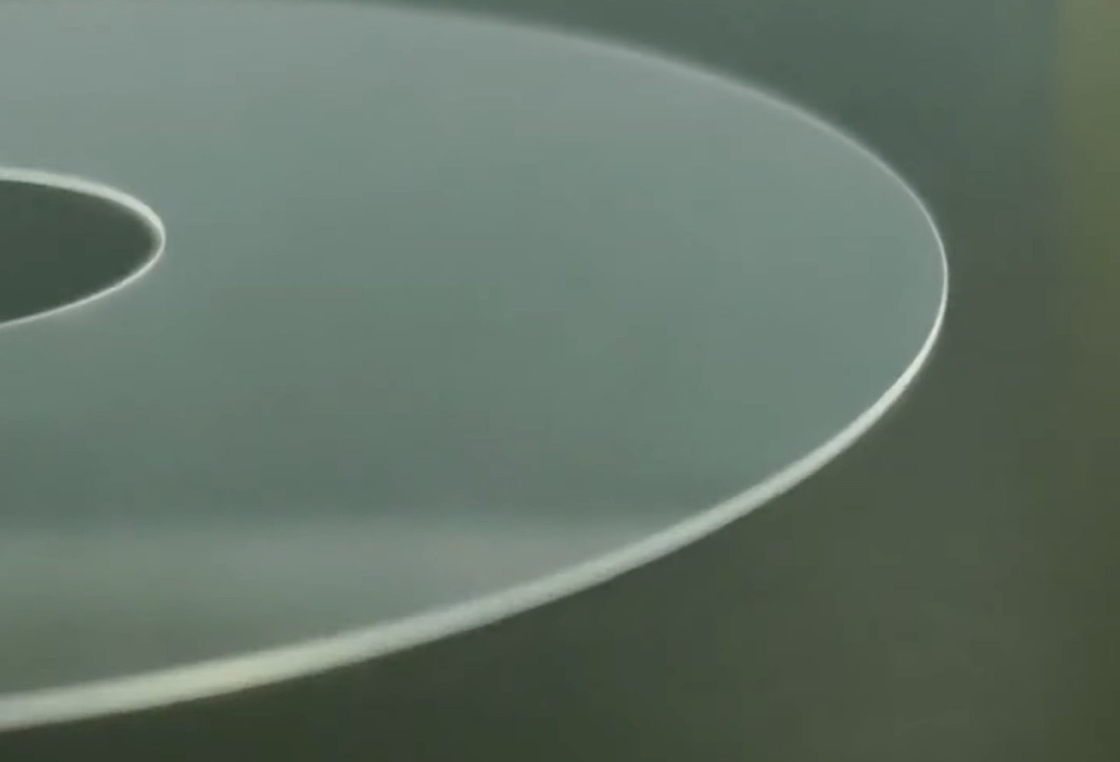
GlaCE™ cuts thin glass and forms its finished, chamfered edge in one ultrafast-laser sequence. It started on the glass platters of next-generation hard disk drives. The same edge problem now limits co-packaged optics and glass-core semiconductor packaging.
Toshiba verified 12-disk stacking in October 2025 by moving from aluminium to thinner glass substrates, and targets 40 TB-class drives in 2027.1
Photonics
Co-packaged optics entered mass production in 2026. NVIDIA began shipping Spectrum-X CPO switches and Broadcom its 51.2T Bailly switch; TrendForce expects volume ramp in 2027–2028.2
Semiconductor
Glass-core substrates are reaching pilot and early production. Absolics targets mass production by the end of 2026, Samsung Electro-Mechanics a plant in H2 2027, and TSMC’s panel-level CoPoS mass production in H2 2028.3
How a project runs
From your glass to a production decision
Mutual NDA
Two signatures, then we share sample data and the details behind this site.
Samples on your glass
We process your glass or parts on our prototype platform in Taiwan.
Your evaluation
Your lab measures; we review the results with your engineers.
Equipment or licence
Production equipment, process licensing or joint development, depending on fit.
High-capacity drives are moving from aluminium to glass platters, and each new design stacks more, thinner platters. The thinner the glass, the more its edge decides strength and yield. GlaCE™ forms that edge without grinding.
Thinner glass, same flaw
Glass fails at its largest flaw. Mechanical scribing, grinding and chamfering remove material by brittle micro-fracture. The visible chips are the smaller part; median and lateral cracks sit below the finished surface and set the weak tail of the strength distribution.
More platters per drive means thinner substrates: the 0.455 mm class today, moving toward the 0.381 mm class. The same edge flaw then takes a larger share of the section, while clamping, spin and handling loads stay.
Seagate’s HAMR platform, Mozaic 3+, grows its iron-platinum media on a glass substrate.1
Toshiba verified 12-disk stacking in October 2025, replacing aluminium with a thinner glass substrate; 40 TB-class drives are targeted for 2027.2
The same edge cracks (orange) take a larger share of a thinner section. Schematic.
The target part
A 3.5-inch disk, cut and chamfered on every edge
Schematic. The published study used 97 mm OD × 25 mm ID × 0.455 mm glass disks, with 45° chamfers on the upper and lower corners of both the inner (ID) and outer (OD) edges.
A finished platter blank has four edge corners: upper and lower, on the inner hole and on the outside. Today each is ground and chamfered with diamond tools, in several stations, with coolant and slurry.
GlaCE™ forms all four in one fixture. The inner and outer edges share one axis of rotation, so their concentricity comes from the setup rather than from repeated alignment.
The process
Three laser stages, one fixture
Bottom chamfer
Ultrafast-laser ablation from the underside forms the lower 45° chamfer.
Vertical cut
A single-pass filament through the full thickness defines the inner and outer separation boundary.
Top chamfer
The upper chamfer is formed after the cut, so the cut track stops any crack before it reaches the bulk.
No grinding wheels, slurry or chemical etch in the forming step. The three-stage sequence is published in Manufacturing Letters 49 (2026).3 The production process window is held as a trade secret.
Scope
What GlaCE changes, and what it leaves alone
Step in a glass-disk flow
With GlaCE™
Core and outer-diameter cut
Replaced laser cut
Inner and outer diameter grinding
Replaced
Edge chamfering, both faces
Replaced laser-formed 45° chamfers
Edge polish
Retained today a laser edge-polish step is in development
Main-surface lapping, polishing and CMP
Not touched
Media deposition and glass composition
Not touched
GlaCE™ changes how the edge is made. It does not change the data surface, the coating or the glass.
Published results
What the papers report
Result
Value
Source
Defect classes for laser-cut glass edges
3: inner cracking, residue, inner chipping
Manuf. Lett. 2026
Inner cracks, 3rd-generation process
15–35 µm
Manuf. Lett. 2026
Inner cracks, 4th-generation process
None
Manuf. Lett. 2026
Edges with chips or cracks above threshold (ten disks, optical microscope)
0 of 40
J. Appl. Phys. 2026
Longest residual surface feature (SEM, 10,000×)
≤ 1.6 µm long, < 0.3 µm wide, < 1% of the face
J. Appl. Phys. 2026
Roughness of the laser-cut face
Sa 0.36 µm
Manuf. Lett. 2026
Operational threshold: no crack 0.5 µm or wider, or 5 µm or longer.4
Seeing the edge
Microscope and SEM evidence
Select any image to enlarge it.
Same glass, same laser: an earlier edge (left) with micro-cracks and chipping, and the GlaCE™ edge (right). Optical microscope, 50 µm bars. J. Appl. Phys. 140, 123110, Fig. 6.Chamfer face at 2,000× with a 10,000× inset: the longest hairline is 1.6 µm, on under 1% of the face. J. Appl. Phys., Fig. 11.Cross-section, 200×: top chamfer, cut wall and bottom chamfer from one process. J. Appl. Phys., Fig. 9.Chamfer face, 1,000×: uniform ablation texture and no edge chipping. J. Appl. Phys., Fig. 10.4th-generation edges, inner (ID) and outer (OD): top chamfer, cut wall, bottom chamfer. Manuf. Lett. 49, Fig. 4.
Latest samples · July 2026
Fifth generation, under production conditions
Inner edge (ID), 100×Outer edge (OD), 100×Cut wall, 2,000×ID chamfer face, 10,000×: smooth, rounded ablation texture; no hairline cracks visible in this field.
Representative SEM views of the three-stage process: the cut wall with the chamfered areas on each side.
Where the program stands
Multi-round sample evaluation with a Tier-1 global HDD manufacturer, with its engineering, sourcing and business teams engaged.
Prototype platform running in Taiwan with our equipment development partner; production tools follow customer qualification.
Fifth-generation images show morphology only; batch statistics on this generation are in progress.
GlaCE Plus Photonics · co-packaged optics In development
Glass parts that hold fibers in place
Co-packaged optics moves the optical engine next to the switch chip. Every fiber must then meet the photonic chip with sub-micron accuracy, at volume. Glass is the natural material for the parts that hold those fibers, and the edge and hole quality that matters on an HDD platter matters here too.
The market
Co-packaged optics reached mass production in 2026
NVIDIA
Began shipping its Spectrum-X CPO switch to select partners. It is built with TSMC’s COUPE packaging and offers up to 400 Tb/s of switching capacity.1
Broadcom
Its 51.2T Bailly CPO switch is in volume manufacturing with Delta Electronics and Micas Networks, and uses up to 70% less power than pluggable transceivers.1
Outlook
TrendForce expects the CPO switch market to reach volume ramp in 2027–2028, with optical-engine yield and advanced-packaging capacity as the bottlenecks.1
Where fiber attach gets hard
Alignment
Single-mode fibers have to sit within a fraction of a micrometre of the chip’s couplers, for every channel.
Assembly time
Aligning each array while measuring light through it is slow and costly as fiber counts grow.
Adhesives
Epoxy shrinkage and ageing can move fibers after alignment and make rework difficult.
Service
A permanent attach makes it hard to test a module or replace a fiber.
What we bring
The same ultrafast-laser platform that forms crack-free glass edges for HDD media also forms edges and holes in thin glass parts, with control of the beam’s angle to the surface.
We are developing glass-based fiber-attach parts for co-packaged optics with photonics partners. Designs, data and patent status are shared under NDA.
GlaCE Plus Semi · glass-core packaging Feasibility
Crack-free edges for glass-core substrates
Glass cores bring flatness, dimensional stability and fine through-glass vias to large AI packages. Their weak point is the same as an HDD platter’s: glass chips and cracks at its edges during drilling and dicing.
The roadmap
Publicly reported status, 2026
Company
Status as publicly reported
Absolics (SKC)
Mass-production samples in Q1 2026 and customer qualification; mass production targeted by the end of 2026, phase-1 capacity 12,000 m² a year.1
Intel
Showed a thick-core glass substrate with embedded EMIB bridges at NEPCON Japan in January 2026 and reported no micro-cracking (“SeWaRe”) issues in testing; TrendForce places commercialization around 2030.1,2
Intel with 3D Glass Solutions
About US$3.3 billion substrate plant in Odisha, India, with a five-to-six-year buildout, per the Indian government.3
Samsung Electro-Mechanics
GLASEM joint venture with Dongwoo Fine-Chem formed in July 2026; Pyeongtaek plant targeted for H2 2027.1
LG Innotek
Prototypes delivered in 2024; production targeted for 2027–2028.1
TSMC
Panel-level CoPoS pilot in 2027 and mass production in H2 2028; glass integration still under review.1
Dai Nippon Printing
Pilot operation since December 2025; mass production targeted for FY2028.1
The edge, in public reporting
Glass chips and cracks at the edges during drilling and dicing.1
Early production runs at one maker reportedly broke hundreds of panels every couple of days (MIT Technology Review, March 2026, via Tom’s Hardware).1
An edge coating reduced measured edge stress from 95 MPa to 49 MPa: the industry is treating the edge after the cut.1
GlaCE Plus forms the cut and its chamfers in one pass, so the edge leaves the singulation step without the crack population that coatings are added to contain.
Panel singulation: cut and chamfer in one pass; amber marks the processed edge.Dicing-street cross-section: chamfers on both faces, formed during the cut.
Singulated unit, package-ready edges.Through-glass via and hole edges.
Edge clearance is wiring area
How much of a unit the keep-out band costs
Designers keep circuits away from a unit’s edge to allow for singulation damage. Published glass-core build-up pull-backs are mostly 50–150 µm,4 and finite-element work has used about 300 µm for via-to-edge distance.5 Every micrometre of that band is area that cannot carry wiring. A cleaner edge lets it shrink.
+10.9% routable area
Routable share of the unit: 88.4% → 98.0%
Keep-out band today Boundary with a cleaner edge
Illustrative geometry for a square unit: routable fraction = (1 − 2w / L)². Not measured data.
Where the program stands
Edge metrics measured on annular borosilicate coupons; transfer to package glass cores is being verified.
Paper accepted at IEEE EDAPS 2026, 14–16 December, IIT Ropar, India.
Looking for substrate makers and OSATs with glass panels or units to process.
We publish the physics and the results. The production process window stays a trade secret.
Publications
Manufacturing Letters 49 (2026) 87–92 · published
Zero-crack laser singulation of thin glass disks for next-generation hard disk drives: a three-stage hybrid ultrafast process
S.-J. Liu, Y.-W. Wang
The three-stage process (bottom chamfer, vertical cut, top chamfer) on 0.455 mm glass disks, a three-category classification of laser edge defects, and the elimination of inner cracks from the 3rd to the 4th generation.
Journal of Applied Physics 140, 123110 (2026) · published
Physics-based damage prediction index model and angle-matched ultrafast-laser chamfering of amorphous glass substrates
S.-J. Liu, Y.-W. Wang
A dimensionless Damage Index predicts where laser-induced cracks start in glass; matching the beam to the chamfer face removed above-threshold cracking on 40 of 40 edges.
Edge clearance in panel-level glass-core substrates: measured damage extent and an interconnect cost model
S.-J. Liu, C.-M. Wang
Measured edge damage on laser-processed glass coupons and what it means for the edge keep-out rule of glass-core packages.
SWTest Asia 2026 · podium · 5–6 November, Hsinchu
Solder-free micro coaxial spring probes for advanced-package test: fluxless fine-spot laser weld characterization and an automated eight-station assembly platform
S.-J. Liu
From Pioneer’s probe business: laser welding applied to test probes for advanced packages.
The physics
Predict the damage, then route around it
Ψ = k0 · M · Φ · P
The Damage Index multiplies four factors: geometry, the glass’s susceptibility, the energy flux that penetrates the bulk, and pulse accumulation. At Ψ = 1 the stress at a flaw reaches the glass’s fracture toughness and cracks start.
The model explains why a laser striking the chamfer wall at the wrong angle drives cracks into the glass, and how delivering it matched to the chamfer face keeps the energy inside the material being removed.2
The three defect classes used as acceptance criteria: inner cracking, residue and inner chipping. Manuf. Lett. 49, Fig. 3.
Pioneer Probe Pins Technology Co., Ltd. is a fabless engineering company in Taiwan with a semiconductor test-probe background: probe cards, test sockets and spring probes. GlaCE™ is its glass laser edge-forming line; the process and IP are developed and owned by Pioneer. PioneerX Holdings, Inc. (Delaware) is the US company.
The name
GlaCE comes from Glass + Chamfered Edge, which is exactly what we deliver: a properly chamfered glass edge. It also happens to be the French word glace (glass, ice), and it reads close to “glass”, so it is easy to say and remember for overseas customers.
IP and brand
Patent applications filed in Taiwan; international filings in progress.
GlaCE™ trademark applications filed in Taiwan for machines, laser processing and R&D services; US filing to follow.
The production process window is held as a trade secret and is never published.
Ways to work together
Four models, chosen per partner
Sample processing
Your glass, our platform, your measurements.
Equipment
Production tools built with our equipment partners, with service.
Process licensing
The GlaCE™ process on qualified platforms.
Joint development
New glass parts and formats with substrate makers, OSATs and photonics companies.
For investors
What is in place
Two peer-reviewed papers on the process and its physics, and a third accepted.
A Tier-1 HDD manufacturer evaluating samples.
A prototype platform running in Taiwan.
Patent and trademark filings; a US holding company.
Business plan, data and terms are shared under NDA.
Contact
Talk to us
Technology, samples and Taiwan
Song-Jhe (Johnny) Liu
Chairman & CEO, Pioneer Probe Pins Technology Co., Ltd. President & CEO, PioneerX Holdings, Inc.
liusj88@gmail.com
Corporate, PioneerX Holdings
Ming Wei (Mark) Hsu
Co-founder and Director, PioneerX Holdings, Inc.
mark.hsu@pioneerxholdings.com
Commercial and partnerships, United States
Eytan Wiener
Potentiate Ventures
Strategic advisor to PioneerX, working with Scott Deetz of Northbound Group.
eytan@potentiateventures.com
General enquiries and sample requests
Pioneer Probe Pins sales
Pioneer Probe Pins Technology Co., Ltd., Taiwan
sales@pioneerprobes.com
Administration, Taiwan
Abby
Pioneer Probe Pins Technology Co., Ltd.
abby@pioneerprobes.com
Pioneer Probe Pins Technology Co., Ltd. · Tamsui, New Taipei City, Taiwan · pioneerprobes.com